IMP Clean room

All resources can be booked on https://www.tuinfra.tu-darmstadt.de/

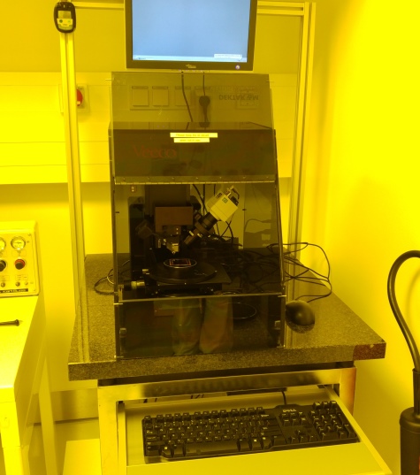
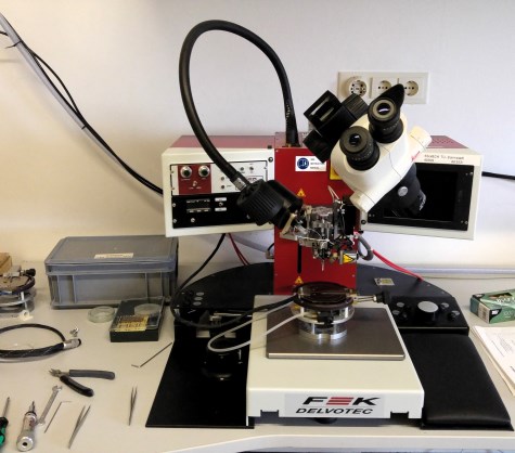
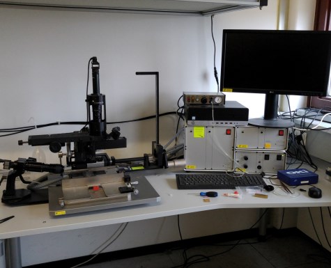
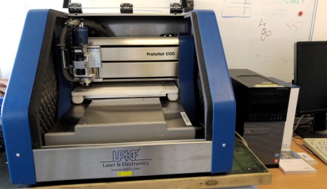
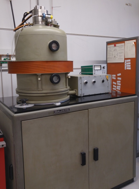
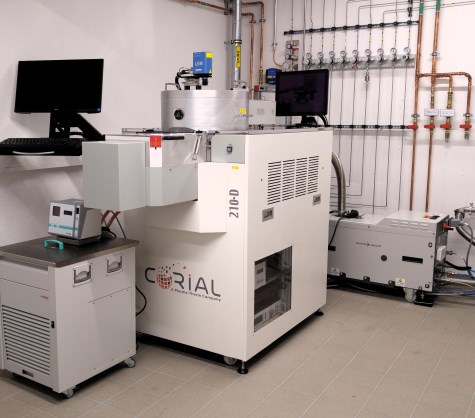
The IMP clean room facilities provide processing technology for structuring and processing of semiconductors, dielectrics and other materials. The technological capabilities also allow for processing microfluidic devices, microwave components and optical components such as Bragg mirrors, amongst others.

More information about specific facilities on the TU Darmstadt website: https://www.tuinfra.tu-darmstadt.de/

A brief Intro to the clean room
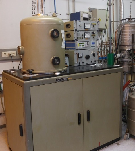
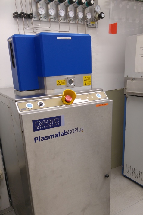
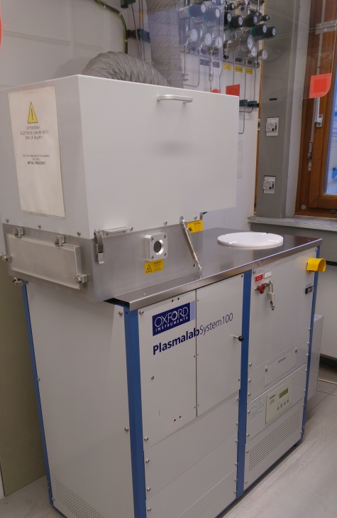
  • E-beam and thermal evaporation system.
  • Possible termal deposition: Au, Ge
  • Possible e-beam deposition: Ni,Ti, Al, Pd, possibly others.
  • Evaporation under an angle possible.
  • Thermal evaporation system.
  • Possible processes: Cr, Au, NiCr

Maximum size 8"

Wire Bonder

Flip chip bonder

Structures printed circuit boards.

Drills contact holes.

Coating with Cr, Ni, Al, Ag

RIE with Ar, CHF3, CF4, O2, SF6, N

PECVD with Ar, Methane, Helium, N2, Silane, Nitrous Oxide, SF6

Deposition of: SiN, SiO and SiC deposition at 80°C.

Ellipsometry for the VIS and NIR

Maximum exposure size 4".

UV-exposure with i-Line (~365 nm)

Maximum exposure size 3".

UV-exposure with i-Line (~365 nm)

Resist coating of wafers and smaller samples

Surface smoothing, e. g. for lapping Gallium Arsenide

Coating thickness and roughness measurement.

Height resolution~5nm

Annealing in quartz tube, vacuum, N2

Annealing up to ~500°C